Positron User Facility
Positron Annihilation Spectroscopy (PAS)
The positron is the antiparticle of the electron. Hypothesized by Paul Dirac in 1928 and discovered by Carl Anderson in 1932, positrons have been used as a powerful and non-destructive probe for materials characterization for decades, especially for studying the vacancy and free volume properties at the atomic level of a wide range of materials. Among the various techniques that use positrons as a probe, Positron Annihilation Lifetime Spectroscopy (PALS) measures the decay lifetime of positrons in the subject materials, which is directly related to the electron density surrounding the annihilating positron and is very sensitive to the concentration and type of vacancy defect and defect clusters.

Another positron technique, Doppler Broadening Spectroscopy (DBS), examines the energy spread of the 511 keV back-to-back annihilation gamma originated from the moving electron when the annihilation occurs. Since the electron energy levels vary in the vicinity of ion cores and vacancies, DBS provides complementary information of the vacancy type and density in the energy domain.
Positron Annihilation Lifetime Spectroscopy
PALS measures the average decay lifetime of positrons upon their first injection into the material of interest. As mentioned earlier, different PAS techniques rely on the detection of annihilation gamma rays and the different aspects of the observed radiations. PALS specifically examines the time scale of the annihilation of positrons, of which the lifetime can be directly correlated to the characteristics of the media they annihilate in. Positrons are stable in vacuum ( > 2×10²¹ years), but once they are injected into normal materials, their lifetimes will be drastically shortened due to their annihilation with electrons in the matter. The behavior of an implanted positron in matter is not simple and straightforward. The process that positrons undergo in solids before they annihilate can be broadly categorized into several time scales: backscattering, thermalization, diffusion, and final annihilation.
In the shortest time scale around 10−15 s, when positrons hit the sample surface, a small fraction is quickly reflected as backscattered positrons. For most of the positrons that are not reflected, immediately after their implantation, the positrons lose most of their kinetic energy by scattering with the host atoms and thermalize rapidly (on the order of pico-seconds). The following diffusion process may result in the trapping of the positrons in defects and voids before their eventual annihilation with the environmental electrons. The positron annihilation lifetime is directly related to the electron density, which is sensitive to the concentration and type of vacancy defects and defect clusters. The lifetime spectrum of positron annihilation is similar to any decay spectrum of radioactive materials with certain half-lives. On a semi-log histogram, the exponential decay component would appear as a straight line with certain slope. A perfect decay spectrum can be expressed as
where is the lifetime of the component, and is the corresponding intensity. A typical PALS spectrum is shown below, which consists of at least two lifetimes convolved with the spectrometer’s time resolution. The shortest lifetime(s) is less than 0.5 ns and is due to the fast positron annihilation. The longer lifetime is due to the annihilation of ortho-Positronium (or o-Ps, a metastable bound state of a positron and an electron) that is typically seen in insulating materials, but not in metals. Note that in the figure below, the random background noise is subtracted, and the peak of the spectrum is normalized to 1.

More generally, the resolution of a spectrum is determined by a number of factors. In our fitting routine, the prompt peak is described as a Gaussian function (of certain FWHM) with different left- and right-hand exponential flanks, which are designated by and , respectively. The bulk PALS system typically shows a FWHM of ~170 ps and /, of ~35 ps. Using POSFIT, the shortest lifetime we normally fit is approximately 100-200 ps. The second lifetime is normally ~300-500 ps after subtracting the source term. These two components in metals can be observed quite ubiquitously and are typically related to the positron annihilation in small (e.g. dislocations, mono-vacancies) and big vacancies (e.g. vacancy clusters), respectively. Sometimes the shortest lifetime can also be a result of delocalized positrons annihilating in the perfect lattice without being trapped in a particular kind of defects. In general, the positron lifetime in a lattice or certain type of vacancies can be theoretically predicted and experimentally examined under ideal conditions. However, there is no universal correlation among different metallic materials since the positron lifetime is sensitive to the particular electronic environment (or chemistry) during its annihilation.
In the figure above, it is also obvious that there is a long lifetime component distinctive from the fast prompt peak and is marked as o-Ps lifetime. This lifetime component is critical in many PALS studies involving insulating materials where o-Ps are readily formed. The o-Ps trapped and annihilate in a free volume void can be straightforwardly treated as a neutral particle in a quantum well, and its lifetime is not sensitive to the electrical and chemical environment. Consequently, the o-Ps lifetime can be related to the size of the quantum well, or the pore size, using a well-established Tao-Eldrup model, where R is in Å, and in ns.
The Tao-Eldrup model has been widely used to calibrate the size of free volumes ranging from several angstroms to a couple of nanometers in polymers. With even larger pores, the Tao-Eldrup model is modified and extended to account for other excited quantum states of the o-Ps that could populate such pores. The extended Tao-Eldrup model can be used to calibrate pore sizes of up to tens of nanometers in diameter.
Doppler Broadening Spectroscopy
Unlike PALS focusing on the time domain of the positron annihilation process, Doppler Broadening Spectroscopy (DBS) of positron annihilation examines the energy spread of the 511 keV annihilation gamma rays due to the momentum of the annihilating electron when the annihilation occurs. The decay energy shift can be detected by a high-resolution detector, usually a high purity Germanium (HPGe) detector, down to several eV from the 511 keV peak. Because the positron rapidly thermalizes after its implantation, the Doppler shift, ΔE, is largely caused by electron momentum which becomes a telltale sign of the characteristics of the annihilation sites. In general, positrons tend to diffuse and be trapped into vacancy-type defects and open volumes of materials to achieve a lower potential energy. Since the electron energy levels vary in the vicinity of ion cores and vacancies, the annihilation of trapped positrons with surrounding low-momentum valence electrons becomes more likely. Under such conditions, the Doppler broadening effect is reduced, and the annihilation peak is narrower. As such, DBS provides complementary information of the vacancy type and density in the energy domain and has been widely used to characterize defects in metal and semiconductor materials for decades. A typical DBS spectrum taken by an HPGe detector is shown in the figure below where multiple energy peaks can be found that correspond to different decay processes. The most prominent and interested peak is the 511 keV peak, which is due to the annihilation of the positrons.

To quantify the Doppler broadening in an energy spectrum of annihilation events, a line shape parameter is introduced. The DBS spectrum is normally Gaussian-like, and a peak region around 511 keV and two wing regions are customarily distinguished by defining an S and W parameter. The S parameter (see figure below) is defined as the ratio of number of events in the center region (shaded) to the total counts of the 511 keV peak, which is a straightforward way of measuring the broadening of the 511 keV energy peak. Positrons trapped in vacancies have much less chance of annihilating with core electrons that have higher momentum, which means the energy broadening of the trapped positrons will be smaller, consequently resulting a narrower 511 keV peak. A simple rule of thumb is that a higher concentration of vacancies traps more positrons and generates a higher S parameter.

Depth-Profiled Positron Annihilation Spectroscopy
One unique and crucially important feature of beam-based PALS and DBS is the depth profiling capability. Traditional PALS and DBS use 22Na directly as the positron source that emits high energy positrons with a wide energy spread and are only suitable for studying thick (millimeter range) materials. The advent of mono-energetic positron beams with controllable positron implantation depth enabled the study of thin films, surfaces, and interfaces. In particular, beam-based positron spectroscopies have demonstrated extensive utility in characterizing very thin films (tens to hundreds of nanometers) on thick substrates. Furthermore, by implanting positrons into different depths into materials, one has the capability of studying the characteristics of inhomogeneous materials and other depth-dependent properties that are localized or heterogeneous.
The positron penetration depth, which is also called stopping depth, depends on both the positron initial energy, E, and the material density, . This stopping distribution has been studied by both Monte Carlo simulations and by many experiments. If a uniform and continuous material is considered, the implantation profile as a function of depth z can be estimated as a Makhovian distribution with different coefficients at different energies. The depth dependence function is,
where is the positron mean implantation/stopping depth in nm,
given the positron energy, E in keV, and the material density, in g/cm3. The depth profile of positrons determined by the Makhovian distribution is a bell-shaped distribution with its maximum at ∼ with FWHM ∼. The Makhovian distributions of positrons at different energies, from 1 keV to 5 keV, are shown in the figure below. As is clearly seen at low energies, the distribution is narrow and close to the film surface, which means excellent resolution to near-surface features. As implantation energies increase, the positron distribution becomes broader and extends deeper into the material. It roughly extends from the surface of the film to twice as deep as the mean implantation depth. Positron beams, like the one at the NCSU PULSTAR reactor, would tremendously facilitate the use of PALS and DBS techniques in materials defect/vacancy characterizations, especially in data extensive and/or time restraining situations.

Intense Positron Beam User Facility
Traditional PAS use 22Na as a typical positron source, which emits positrons with a relatively high energy and wide energy spread. It is suitable for studying bulk materials with thicknesses of several hundred micrometers to millimeters. The advent of low energy positron beams with controllable positron implantation depth enabled the study of thin films, surfaces, interfaces, and other depth-dependent properties. The technique showed great success in materials characterization and tremendous potential of advancing our understandings of some fundamental problems with its unique perspective.
The prevalence of the positron techniques, however, is limited by the availability of positron sources to general users. In 2009, as an effort to address this issue, an intense positron beam facility has been established at the North Carolina State University (NCSU) PULSTAR nuclear reactor. Two positron annihilation spectrometers associated to the main beam have been built and tested. The facility provides not only high intensity positron sources, but also a suite of positron characterization capabilities and associated technical support to facilitate easier access to the facility for the users. A schematic of the intense beam user facility is shown below.

Intense Positron Source
At the NC State University PULSTAR Reactor laboratory, the intense positron source (IPS) is comprised of a Platinum moderator assembly surrounded by a Cadmium shroud located adjacent to the PULSTAR core in beamport #6. Positrons are created when gamma rays emanating from the reactor, and from neutron capture in the Cadmium shroud, interact via pair production with the Platinum nuclei. Positrons emitted from the Platinum with kinetic energies of a few eV are accelerated and focused electrostatically into a magnetic field for transport out of the bio-shield. The IPS delivers a 25 mm diameter beam with an energy of 1 keV and intensity of ~6×10⁸ positrons/second. A picture of a Platinum converter bank and schematic of the IPS structure and its picture are shown below.

(Middle) A schematic of the positron generator and the beam head structure.
(Right) The assembled beam head with 4 moderator banks and the electrostatic lenses.
Positron Spectrometers
With magnetic guidance, the primary positron beam is subsequently transported out of the high radiation area through magnetic switches and into adjacent labs that house two positron annihilation spectrometers. These spectrometers are both set up to conduct positron annihilation lifetime spectroscopy (PALS) and Doppler Broadening Spectroscopy (DBS) of annihilation irradiation, mainly used as a nanomaterial characterization tool for users. Other positron methodologies could also be implemented per users’ request.
The e+-PAS Spectrometer
The e+-PAS Spectrometer
The first spectrometer, namely the e+-PAS, uses RF electric fields to bunch positrons into sub-nanosecond pulses when running in PALS mode and is suitable for lifetime studies in materials such as semiconductors and metals. A schematic and picture of this spectrometer are shown below.
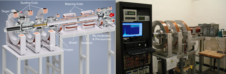
In the e+-PAS, a transmission remoderator made of a 150 nm thick and 10 mm in diameter Nickel foil refines the phase space of the incoming primary beam and also, in combination with a high-transmission mesh, acts as a pre-buncher fed with a 50MHz sawtooth wave to re-emit the positrons in pulses. The pre-bunched positron beam is accelerated by electrostatic lenses and magnetically guided to the entrance of the buncher. Between the pre-buncher and the buncher, steering coils are used to deflect the beam around an internal lead shield that minimizes the target background due to positron annihilation at the remoderator. In addition, a high-transmission mesh acting as a chopper is positioned in front of the main buncher to minimize the background positrons that are misaligned in time domain with the buncher. Subsequently, the beam is fed into a double gap buncher operating at 50 MHz compresses the width of the beam pulses in the time domain. The positrons exit the buncher in phase with the sine wave and travel through another drift tube and arrive at the sample surface with an optimized time focusing. The sample bias can be adjusted from 0.5 keV to 30 keV, which correspond to mean implantation depths of approximately 13 nm to 9 μm assuming the density of the material is 1 g/cm3. Given the routinely achievable positron rate of 5×10⁸ e+/s, the on-target positron rate is approximately 6×10⁵ e+/s considering the loss during the process of transporting, bunching, and re-moderating the beam. The pulsed spectrometer has a superior timing resolution of approximately 280 ps, which resolves short positron lifetimes in metals and traditional semiconductors. The beam spot size is approximately 10 mm.
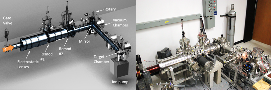
The Ps-PAS Spectrometer
The Ps-PAS spectrometer uses secondary electrons from the target for timing (1 ns time resolution) and is used to measure positronium lifetimes and to study free volumes and morphology in nano-porous materials. The Ps-PAS spectrometer is electrostatically focused with two remoderators using 150 nm thick Nickel foils. A microchannel plate (MCP) with a center hole is positioned in front of the target to detect the secondary electrons emitted from the sample surface and used as the spectroscopic start signal. Due to the variation in time when the secondary electrons arrive at the MCP, the timing resolution of this spectrometer is limited to ~1 ns. Comparing to the pulsed positron spectrometer, this spectrometer has a much wider timing window of 1000 ns. The Ps-PAS is currently being upgraded to obtain sub-millimeter beam spot size (from several mm) so that the instrument can be used for the characterization of small samples and subsequently obtain spatial resolution along the surface of a sample in the future. In-situ thermal treatment from cryogenic temperature to 500°C can also be done in this spectrometer with its heating-cooling sample stage.
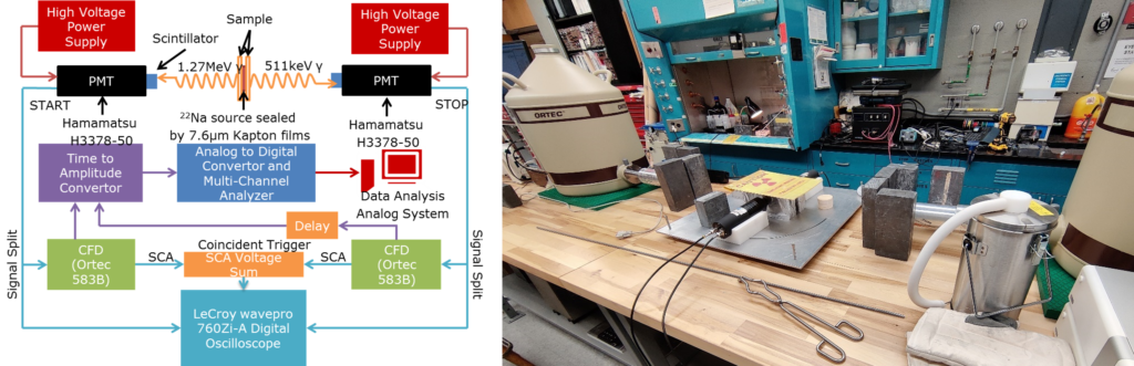
The Bulk PAS Spectrometer
In addition to the beam-based spectrometers described above, a Na-22 based bulk PAS system is also currently operational at the PULSTAR reactor. A schematic and a picture of this system are illustrated below. This system has complete digital signal processing and data acquisition enabled by a LeCroy WavePro 760Zi-A digital oscilloscope. The source-sample package can be placed on a heating-cooling stage inside a vacuum chamber. The temperature of thermal treatment to the sample ranges from approximately 80K to 600K. The sample stage is positioned in between two Hamamatsu H3378-50 photomultiplier tube (PMT) assemblies in combination with two sylindrical plastic scintillators of 1 inch ×1 inch in size. This system has <200 ps time resolution together with the capability of conducting environmental experiments at controlled humidities (0–100%), pressure (vacuum–14 atm), and temperature (cryogenic–1000°C). This system can be used for the study of vacancy, vacancy cluster, or void concentration and size, etc. in various types of materials of millimeter level thickness. Coincidence Doppler Broadening (CDBS) systems have also been implemented in both the e+-PAS and the bulk spectrometers using digital MCAs.
Applications of Positrons
The physical property of the positron enables its application as a unique and nondestructive probe for materials characterization, especially the detection of the atomic-level open spaces, e.g. vacancies, free volumes, and voids, in condensed matter. In our facility, these measurements include, but not limited to, depth-profiled PAS on inhomogeneous vacancy, pore structure, and morphology that are intrinsic to materials, e.g. polymers, nanocomposites, thin films, membranes, and/or introduced by specific procedures (thermal, mechanical, electrical, radiation, adsorption, etc.). Additionally, in-situ measurement using the positron as a probe during these processes is another major advantage of the PAS techniques.
Radiation Damage & Nuclear Materials
Evolution of radiation induced damage caused by neutrons and other high energy particles, of which the characterization and quantification pose tremendous challenges to some of the traditional techniques.

- Single Vacancies & Point Defects
- Nano-Void Nucleation
- Helium Bubble Formation
- Solute Segregation & Precipitation
- Dislocation Loops & Networks
- Free Volume in Amorphous Materials
Semiconductors & Optoelectronics
Identification of “killer” defects that limit charge carrier lifetime and device efficiency
- Cation/Anion Vacancy Complexes
- Dopant-Vacancy Interaction
- Interface State Characterization
- Non-Stoichiometry & Native Defects
- Deep-Level Defect Mapping
Polymers & Soft Matter
Measuring “Free Volume” (FV) holes that dictate mechanical and transport properties.

- Free Volume Hole Size Distribution
- Glass Transition (Tg) Dynamics
- Crystallinity & Phase Separation
- Physical Aging & Structural Relaxation
- Permeability & Diffusion Pathways
Metals & Structural Alloys
Early-stage detection of mechanical failure and alloy phase stability
- Dislocation Density & Forest Hardening
- Pre-Precipitation (GP Zones)
- Hydrogen-Defect Interaction
- Grain Boundary Segregation
- Amorphous-to-Crystalline Transitions
We welcome requests for measurements and collaborations from both academic institutions and industrial partners. Please contact the Manager of Nuclear Services if you are interested in learning more about applications of the positron spectrometers.
Select Publications
Facility Publications
- M. Liu, Y. Akter, A. Bauyrzhan, A. I. Hawari, “The Positron User Facility at the PULSTAR Nuclear Reactor Applications in Materials Studies and Recent Upgrades”; Solid State Phenomena, 374, 155, 2025
- M. Liu, A. I. Hawari, The upgraded intense positron beam facility at the PULSTAR reactor; AIP Conference Proceedings, 2182, 040008, 2019
- M. Liu, J. Moxom, A. I. Hawari, D. W. Gidley, The intense slow positron beam facility at the PULSTAR reactor and applications in nano-materials study, AIP Conference Proceedings 1525 (1), 455-459, 2013
- A. Hawari, D. Gidley, J. Xu, J. Moxom, A. Hathaway, B. Brown, R. Vallery; “The Intense Slow Positron Beam Facility at the NC State University PULSTAR Reactor”; Application of Accelerators in Research and Industry; 20th International Conference; 2009
- J. Moxom, A. Hathaway, A. Hawari, Member, IEEE; “Out of Core Testing of the North Carolina State University PULSTAR Positron Beam”; 2007 IEEE Nuclear Science Symposium Conference Record
- D. Gidley, H. Peng, R. Vallery; “Positron Annihilation as a Method To Characterize Porous Materials”; Annual Review of Materials Research; 2006
User Publications
- Wall, James J., et al. “Irradiation of ultrasonic sensors and adhesive couplants for application in light water reactor primary loop piping and components.” Nuclear Engineering and Design 414 (2023): 112594.
- Burba, Christopher M., et al. “The Effect of Fluorinated Solvents on the Physicochemical Properties, Ionic Association, and Free Volume of a Prototypical Solvate Ionic Liquid.” ChemPhysChem 23.4 (2022): e202100548.
- Wu, Yuntao, et al. “Role of lithium codoping in enhancing the scintillation yield of aluminate garnets.” Physical Review Applied 13.6 (2020): 064060.
- Yang, G., et al. “Material defect study of thallium lead iodide (TlPbI3) crystals for radiation detector applications.” Nuclear Instruments and Methods in Physics Research Section A: Accelerators, Spectrometers, Detectors and Associated Equipment 954 (2020): 161516.
- Zhou, Hanhan, et al. “Radiation-induced changes of vacancy-type defects in ferroelectric capacitors as revealed by Doppler broadening positron annihilation spectroscopy.” Journal of Applied Physics 124.24 (2018).
- Torstensen, Jonathan Ø., et al. “Swelling and free-volume characteristics of TEMPO-oxidized cellulose nanofibril films.” Biomacromolecules 19.3 (2018): 1016-1025.
- Mineart, K. P., et al. “Molecular and morphological characterization of midblock-sulfonated styrenic triblock copolymers“, Journal of Polymer Science. Part B, Polymer Physics, 55(6), 490-497.
- Goshima, Hiroshika, et al. “Addition of monovalent electrolytes to improve storage stability of freeze-dried protein formulations.” Journal of Pharmaceutical Sciences 105.2 (2016): 530-541.
- Nandi, Shyamapada, et al. “A single-ligand ultra-microporous MOF for precombustion CO2 capture and hydrogen purification.” Science advances 1.11 (2015): e1500421.